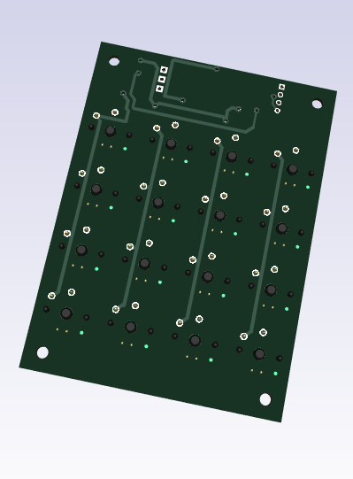
Double sided pcbs with KiCad, pcb2gcode and bCNC.
Designing in KiCad
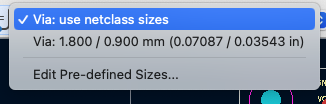
Set your design rules to 0.4mm min track, 0.25mm spacing. Make your vias 2.4mm (1.8mm at minimum) with 0.9mm drill (to fit 0.9mm via rivets, if you are using soldered wires for vias you can go smaller).
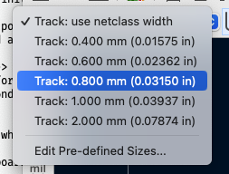
Use the biggest tracks you can fit. 1mm for power, 0.5 or 0.4 for signals. Consider using 0.6 or 0.8 when you can.
Place four 3.175mm holes equidistant from each corner with a 7mm courtyard around the hole. You can get away with two if you can’t afford the space. We are going to use 3.175mm drill bit shanks (you will accumulate a near-infinite collection of broken ones, trust me!) as locator pins.
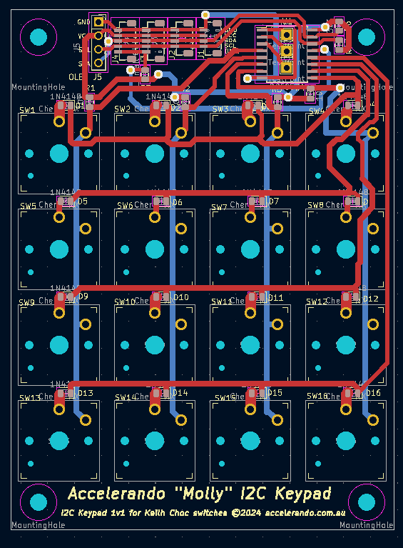

Try to keep tracks vert/horiz where possible (I do front=horz
back=vert, or vice-versa), as this saves milling time versus jinking
the milling head around following complex tracks. In KiCad you can
use the D key to engage track drag mode for removing kinks from
tracks.
If you are aiming for a single sided board or need to run tracks under components, using 1206 size parts (0805 in a pinch) can help. I sometimes design with 0603 and “upsize” parts when I need to route under them.
Generating Gerber files with KiCad
Plot your board in KiCad with File -> Plot. Make sure the Use extended X2 format checkbox is OFF. Generate drill file also;
check the option for Plated and Non-Plated Through-Holes (NPTH) in
same file, even though we want one file for our component holes and a
second file for our locating pins (the non-plated through holes).
We’ll fix this later by copying the drill file and keeping just the
locator holes in the copy.

Converting Gerber to G-Code with pcb2gcode.
PCB2gcode has a GUI but I just use the same config file copied from project to project.
See below my millproject file, which sets which side each operation is done
from. For quick prototypes I try to make single-sided designs where
possible (in which case, set cut-side=front). You can tweak the
tile options to produce multiple copies of a board.
For boards below about 100mm, I’ve found auto-leveling is not necessary. If the board blank has any bow in it, auto leveling corrects for this in software (by adjusting the Z-height to follow the blank).
1 |
|
Run pcb2gode, and note the printed board width.
on No in molly-i2c-macro-keypad on main [!?]
50% ❯ pcb2gcode
Importing front side... DONE.
Importing back side... DONE.
Importing outline... DONE.
Processing input files... DONE.
Exporting back... DONE. (Height: 99.82mm Width: 74.42mm)
Exporting front... DONE. (Height: 99.82mm Width: 74.42mm)
Exporting outline... DONE. (Height: 99.82mm Width: 74.42mm) The board should be cut from the BACK side.
Importing drill... DONE.
Exporting milldrill... Exporting drill... DONE. The board should be drilled from the FRONT side.
END.
We are going to re-run pcb2gcode, giving half this value as a mirro-axis setting. eg if pcb2gcode says Exporting back... DONE. (Height: 99.82mm Width: 74.42mm) this would mean you should run pcb2gcode again giving the option -—mirror-axis=37.21.
You can add the option to your millproject file if you like (remember to update it if you change the board dimensions).
Once you have run pcb2gcode again, using the mirror-axis option, the generated gcode for front and back will now overlap perfectly.
on No in molly-i2c-macro-keypad on main [!?]
50% ❯ pcb2gcode --mirror-axis=37.21
Importing front side... DONE.
Importing back side... DONE.
Importing outline... DONE.
Processing input files... DONE.
Exporting back... DONE. (Height: 99.82mm Width: 74.42mm)
Exporting front... DONE. (Height: 99.82mm Width: 74.42mm)
Exporting outline... DONE. (Height: 99.82mm Width: 74.42mm) The board should be cut from the BACK side.
Importing drill... DONE.
Exporting milldrill... Exporting drill... DONE. The board should be drilled from the FRONT side.
END.
Make gcode for the locator holes
Copy the drills.gcode to locators.gcode. Edit the
locators.gcode file and search for Change tool bit to drill size XXmm. For each
occurence of this message except your locator hole size, delete that block and the following
movement block. When you find the 3.175mm block (the size of our
locator holes), change the Z drill depth to -6mm (you can just global
search and replace “Z-1.8” for “Z-6.”).
Recently, I have had good results using normal 0.9mm holes (for header pins etc) as my locators, by using a 15mm length of 0.8mm stainless steel wire as locator pins.
Find the drill sections for your locator holes:
(MSG, Change tool bit to drill size 3.175mm)
M6      (Tool change.)
M0      (Temporary machine stop.)
M3      (Spindle on clockwise.)
G0 Z1.00000
G04 P1.00000

G1 F100.00000
G0 X6.73000 Y6.73000
G1 Z-2.00000
G1 Z1.00000
Modify the depth to 6mm:
G0 X6.73000 Y6.73000
G1 Z-6.00000
G1 Z1.00000
Holding the PCB blank
Fix your spoilboard to the mill bed so that it will not move (either double-sided tape or recessed T-bolts). I mill a slot in the side of my spoilboard to allow use of low-profile clamps.
You can also just use normal milling clamps to hold both the spoilboard and PCB, if you are careful to remove one clamp at a time and re-clamp the spoilboard when removing the PCB to flip it (and be super careful not to crash into the clamps. I lose more engraving bits that way!).
I use 17mm MDF for a spoilboard, cut on tablesaw into blocks the same size as my PCB blanks, and I re-use the spoilboard board many times until it is not flat.
Clamp the PCB and spoilboard down. If you have autoleveling probe, use it, but I have found that with 0.1mm narrow angle engraving bits this is not super critical, I do not typically use auto leveling. If you’re using a 60degree V-bit, leveling its totally critical.
Zero the X and Y axis at the point where you want the lower left corner of your PCB. You won’t need to alter X and Y, but EVERY time you change a bit you must re-zero the Z axis.
If you have Z-probing, use that to zero the Z-axis. If not, lower the bit until a piece of paper is trapped under it. For isolation set the height to 0.2mm (value may vary depending on type of paper you use, depth comes out wrong, adjust your value). For drilling and outline cutting I just find “paper trapped height” and set that as zero.
Milling the board
You can use whatever G-code sending software your mill supports. My
mill runs the GRBL firmware, and I use the python bCNC gcode
editor and sender.

Start with the FRONT isolation.
A thin film of machine oil smeared over the board with a fingertip will give a vastly improved cut.
Do a SCAN before routing to make sure you wont crash. Then run the front.gcode file, which will isolate tracks. If you’ve used fill zones, you will get a double isolation process.
Drill all the holes from the front
Now do the drilling from the front. You will probably change drill bits several times. Leave whatever last drill you used (say 0.9mm) in place when it comes time to do the corner holes.
Finally put in a 3.175mm bit and run the deepdrills.gcode. You now have holes that will let you flip the board perfectly. This relies on your holes being placed equidistant from the board edge (or centerline) in your design.
Flip the board
Now you can flip the board. It’s important not to move the spoilboard, so either clamp the spoilboard separately, or remove one clamp at a time and replace the clamp underneath the PCB until you have freed the PCB, and then re-clamp the flipped PCB the same way (this is more complicated to type than to do).
Use the locator pins to position the PCB and clamp it down. THEN REMOVE THE PINS. If you leave the pins in you risk breaking a bit if the mill decides to travel over a locator hole. Do an autolevel if you wish.
Cut the back side tracks
Next do the isolation pass on the back side. Before starting, do a border scan and maybe click around using “move gantry” to make sure that if you tell the bit to move to a particular hole on the computer, it it looks like the engraving bit lines up with that hole on the machine.
Cut the board outline
Finally do the outline pass, cutting the board from the panel, except for some bridges.
If you have a bandsaw or guillotine, you may opt to separate the boards using that instead of a milling cutter.
You’re done on the machine. You can undo all the clamps and remove.
Cleaning up the board
Use a quite stiff brush (even brass or stainless steel) to get the phenolic or fiberglass dust out of the routed isolations. Rub the burrs off each side with some 800 grit wet and dry sandpaper. Using water may help to get the dust out of crevices.
Wash the board in warm soapy water if you used oil.
If your cutter is blunt you will get rough edges. If your cutter is new you should have minimal rough edges. Bakelite (phenolic) substrate is very easy on cutters, while FR4 (fiberglass) substrate can blunt a cutter in a single job. If you have very bad burrs, a dremel tool with a stainless cup brush is a good way to tidy up rough edges.

Soldering
When soldering, it really helps to use flux paste from a syringe because normally you are soldering to a pre-tinned board which is much easier compared to bare copper. With flux paste applied soldering becomes pleasant again. Use an extractor fan.
I find pre-tinning one pad for each component makes it easy to solder the first pin, and get the part straight. I mount every part with one pin then go back and do the other pins.
You can use via rivets or short pieces of wire to fill vias. I take about 8 pieces of wire and place them in 8 vias, solder those, cut and do 8 more. Then I flip the board and solder the other sides.
If you have through hole pins that meet tracks on the top side, make sure you solder the pin to the pad on BOTH SIDES. With headers, female headers are much easier to do than male headers, as you can solder the back side, lift the shroud slightly, solder the front side where necessary (I only do this where a track meets a pin), then replace the shroud. Using a vise can help to squeeze the shroud back into place. Make sure to support the pins so that you don’t lift any bottom tracks when pushing the shroud back down. For male header pins, surface mount pins are a better choice.


After soldering, spray the board with protective lacquer.